Showing posts with label nano. Show all posts

Sunday, December 9, 2012

Nano in your Daily Life

Nano became a major trending label in the beginning of the 21st century. Nowadays, you see socks, packages, food, cars, mp3 players, etc. labeled with nano. Nano sells! I want to show you what’s the science behind some of the major nano labels. For this, let me first describe to you very quickly what nanoparticles are and why they are so beneficial.

What are Nanoparticles?
Nanoparticles are small structures with a diameter of 1-100nm. At this length scale, some materials have different properties than in their bigger bulk material. Because these particles are so small, the surface area per volume is much higher. Most reactions usually happen at the surface of a material, therefore, a higher surface area means more reaction happening. Nanoparticles are actually not an invention of the modern world. These particles were around since a long time. However, nowadays these particles are trending and a good selling label.

What are Socks with Silver Nanoparticles?
There are many brands who offer socks enhanced with silver particles. But what exactly do these silver particles do? These silver nanoparticles can kill many different types of bacteria and therefore the smell from your socks. Silver nanoparticles are not only added to the fabric of socks or underwear, but also to food packaging, cosmetics, tooth brushes and even bandages.

Why add Titanium Dioxide to Sunscreen?
Most of the available sunscreens contain titanium dioxide nanoparticles (TiO2) or zinc oxide (ZnO). These specific nanoparticles are added to sunscreens as they block ultraviolet (UV) light very efficiently. Usually, the higher the blocking factor of your sunscreen, the whiter the sunscreen appears. However, if you shrink the size of titanium dioxide to the nano size, these particles are transparent and can therefore be added to light sunscreens without the thickening white effect.

Are Nanoparticles dangerous?
There is a strong debate whether particles are harmfull to your body or not. Many believe, that due to their small size they can enter into parts of your body, where you do not want to have any other materials. One can not say that nanoparticles in general are dangerous, as these properties differ very strongly among different types. There is a lot of research going on to measure the effect of nanosized particles to our bodies and environment. But don't worry, most countries have very strict regulations about putting nanoparticles into the market. 

Thursday, October 4, 2012

What is a cleanroom and why do you wear these funny white overalls?

Ever wondered how your cell phone camera sensor is build or the processor in your computer? These tiny but incredibly powerful sensors are fabricated in clean rooms, or so called fabs (short for microfabrication, the process done in cleanrooms). What is a fab? Its not just a room which is being cleaned often. You can not just enter this kind of room without preparing yourself for it. In principle it is a room which has way less dust particles in the air than every other room. In the average environment there are about 35,000,000 dust particles flying in 1 cubic meter. However, if you enter an average fab, there are only 3,500 particles in the same area! In high class fabs you will even only have about 35 particles in 1 cubic meter. Some of the questions that I'm trying to answer in this post are, how do you get rid of all the dust, how do you keep it clean and most importantly why do we need fabs in the first place?
Why? Clean rooms in general are used to manufacture small, complicated and delicate sensors, e.g, CMOS chips (the camera sensor in your cell phone), gyroscopes (the thing that makes your screen turn on your cell phone) or computer processors. All of these sensors feature very small parts and electronic circuits. These tiny structures are usually only a few micrometer or even smaller in size, some features are in the nanometer scale, current processors have 22 nm features. The sensors are fabricated on single crystal silicon wafers, which are round thin plates with a size of 4 to 12 inch. Multilayer coating, etching and developing steps are done to fabricate these sensors. Several dozens or hundreds of sensors are fabricated at once on one of these wafers and are cut afterwards. Due to the fact, that these chips have small features one dust particle alone can block a channel, gap or pixel in the case of the CMOS. The whole chip can be ruined afterwards. Therefore, the fewer particles in the air, the better the yield from one wafer and the lower the cost.

How to achieve a clean environment? Clean rooms are expensive facilities used in industry, research facilities or universities. The basic idea of a clean room is to have a constant air flow coming from the ceiling going straight down to the ground. In high end fabs, the floor is made from tiles with tiny holes, so air can flow through. This way any dust particles which happen to flow in the air are forced downwards and will be sucked by the ground. Another method is to suck the air from the sides in the floor. Of course, the air which is blown from the ceiling needs to be filtered first, so no particles are blown in the room at the first place. Once you have a clean environment, several procedures need to be taken to maintain the cleanliness. The air flow in the fab is crucial, therefore you shouldn’t move too fast in a fab, as dust particles on the floor might be whirled up. 

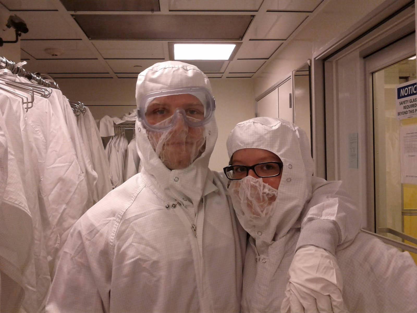
What are the precautions to take before entering a clean room? Humans bring in most of the contamination into a fab, all the dust from your clothes will ruin the clean room. Therefore, you need to wear a hairnet, a mouth protection, a hood, gloves, shoes and a protective overall. Depending on how 'clean' the clean room is, you’re now ready to enter the clean room. However, if you’re about to enter a class 100 fab (cleanroom category indicating less than 3,500 particles per 1 cubic meter), you need to do much more than that. Intel e.g. has a 42 step protocol on how to enter a clean room. One of these steps is to drink a glass of water before entering the fab to clean the throat from any dust, incredible right? Additionally, regular paper, make-up and mechanical pens are not allowed. Some fabs also have a small room which you have to enter first in which all excess dust particles on your body will be blown away by strong air nozzles, it’s like taking an air shower to clean yourself. This is how you might look like before entering a cleanroom. The picture on top shows my brother and me inside the clean room facilities at the Kavli Nanoscience Institute at Caltech, USA. 

Why do most clean rooms look yellow? One main procedure done in fabs is to perform photolithographic steps. It’s similar to taking pictures and developing them in a dark room. However, the wafers will be coated with a photoresist first, which is a light sensitive liquid. Subsequently, a transparency mask with your desired features is laid on top of the wafer and the wafer is exposed to light. Depending on the type of photomask the photoresist will be hardened. Afterwards, you can develop the wafer and the uncrosslinked photoresist will be removed. As the photoresist is light sensitive, yellow light is installed in some parts of the fab, because the photoresist is only sensitive to white light and will not develop under yellow light. 

Overall, clean rooms are awesome and very useful. Without them, we wouldn’t be able to fabricate better, smaller and faster processors. 

Sunday, September 9, 2012

What is ‘Power of Minus 9’?

Power of Minus 9 is a nanotechnology blog which explains the beautiful, mysterious and inspiring world of life in the nano-scale and beyond. This blog intends to explain current nano-related topics to the curious, anxious, attentive future nerds and all others. I want to show you how awesome science can be. 

So, what exactly is the name ‘Power of Minus 9’ referring to? It is an allusion to the scale of a nanometer (nm), which is a billionth of a meter and in scientific terms written as 1*10-9 m, which is 0.000000001 m, a loooot of zeros. This scale is really small, e.g. an atom has a size of 0.1 nm, only a tenth of a nanometer. Amazing, isn’t it? To show you how small a nanometer is, imagine a hair, which is roughly 0.1 mm thick, now cut it into 100’000 pieces then you end up with hair pieces that have a thickness of 1 nm. It’s like looking at stars, but the other way around. Instead of looking extremely far away, you’re looking to the other side of the scale, extremely zoomed in. 

What is all the hype about nano then, except that it’s incredibly small and hard to see, feel or imagine? Well, if you are dealing at this scale, you are trying to understand what single molecules, atoms and cells are doing. Quantum effects play an important role as well, particles do not behave like we used to know anymore. They start to exist at two different places at the same time, a lot of weird stuff is going on down there. Useful applications result out of nanoscience as well, like designing new electronic memories built out of single atoms to enhance performance and decrease size. A more futuristic idea is to fabricate a nano-sized small robot which navigates through your blood system and repairs the human body from the inside.

Principle of Atomic Force Microscopy (AFM). The cantilever
scans over the surface. Due to forces between the atoms
the cantilever will bend and a topography map is created.
What’s different about this scale is how to ‘see’ what you’re dealing with. With a microscope you can’t visualize single atoms; the resolution is by far not high enough. However, there exist several techniques, which allow you to see what atoms look like and are what they are doing. One of them is Atomic Force Microscopy (AFM). It’s a very powerful tool and actually a quite simple technique. You take a cantilever made of silicon, which looks like a long arm attached to a base. At the far end of the cantilever is a tip shaped like a pyramid. Ideally, this tip is very sharp with only one single atom at the end. The tip scans over the surface and senses individual atoms underneath. If there is a valley or a hill, the cantilever will bend towards or away from it. With a laser, which emits light onto the cantilever, the movement can be detected and a topographic map is created (see image). The AFM was invented in the 80s and opened the door to the nanoworld, as this was the first tool to imagine non-conducting surfaces at the nanoscale.

This blog will explain and discuss the latest development in the broader field of nanotechnology, trying to answer questions like, what does a quantum computer do? How does your cell phone camera works? What is a brain chip? What’s up with nanofluidics? and many more. Getting curious? All of these questions will be clarified in a simple but challenging way, so that everyone can have a piece of the awesome nano-cake. If you’re interested in a topic, leave me a comment and I will try my best to cover this in one of my next posts.