“I think I can safely say that nobody understands quantum mechanics.” - R. Feynman (1965)
The strange and wonderful world of quantum mechanics will be the main topic of my first series of blogs. First, I’ll start off with quantum computing, followed by more general topics in quantum mechanics like Schrödinger’s cat. But first, let me start with some basics.
What is the difference between a “normal” computer and a quantum computer? Computers nowadays are based on transistors and handle information using binary bits. These bits can have values of either 0 or 1. Every text or image file is encoded using only 0 or 1. In contradiction, a quantum computer operates using so called qubits (quantum bits). A qubit must have two states, 0 or 1 as well. However, in addition they can also be in a superposition of both, that means in both of them at the same time. You could think of a qubit as an electron. An electron is rotating along it’s axis, which is called spin. The electron’s spin is either directed upwards (spin up) or downwards (spin down). The up or down state is now acting as your 1 or 0. As previously explained, this qubit can also be in a superposition of both.
Why are quantum computers so powerful? The principle of superposition can be scaled with the number of qubits. A computer with two qubits can be in a superposition of 4 states, whereas a classical computer can only be in one of it’s 4 possible states. Because qubits can be in a superposition of both states, the state is rather presented by a probability. There is a certain probability you can find the electron in either of these states. With that you can enhance current processing speeds enormously.
Are their any commercial applications of quantum computing yet? In 2011, a canadian based company, called D-Wave started selling the first commercially available quantum computer. It features a 128 qubit processor which is housed in a cryogenic system. Earlier in 2009, Google demonstrated the use of D-Wave’s technology for image recognition. This brings us a big step forward, however, with a cost of $10,000,000 it’s still a bit pricy for the everyday use.
Sunday, October 28, 2012
Thursday, October 4, 2012
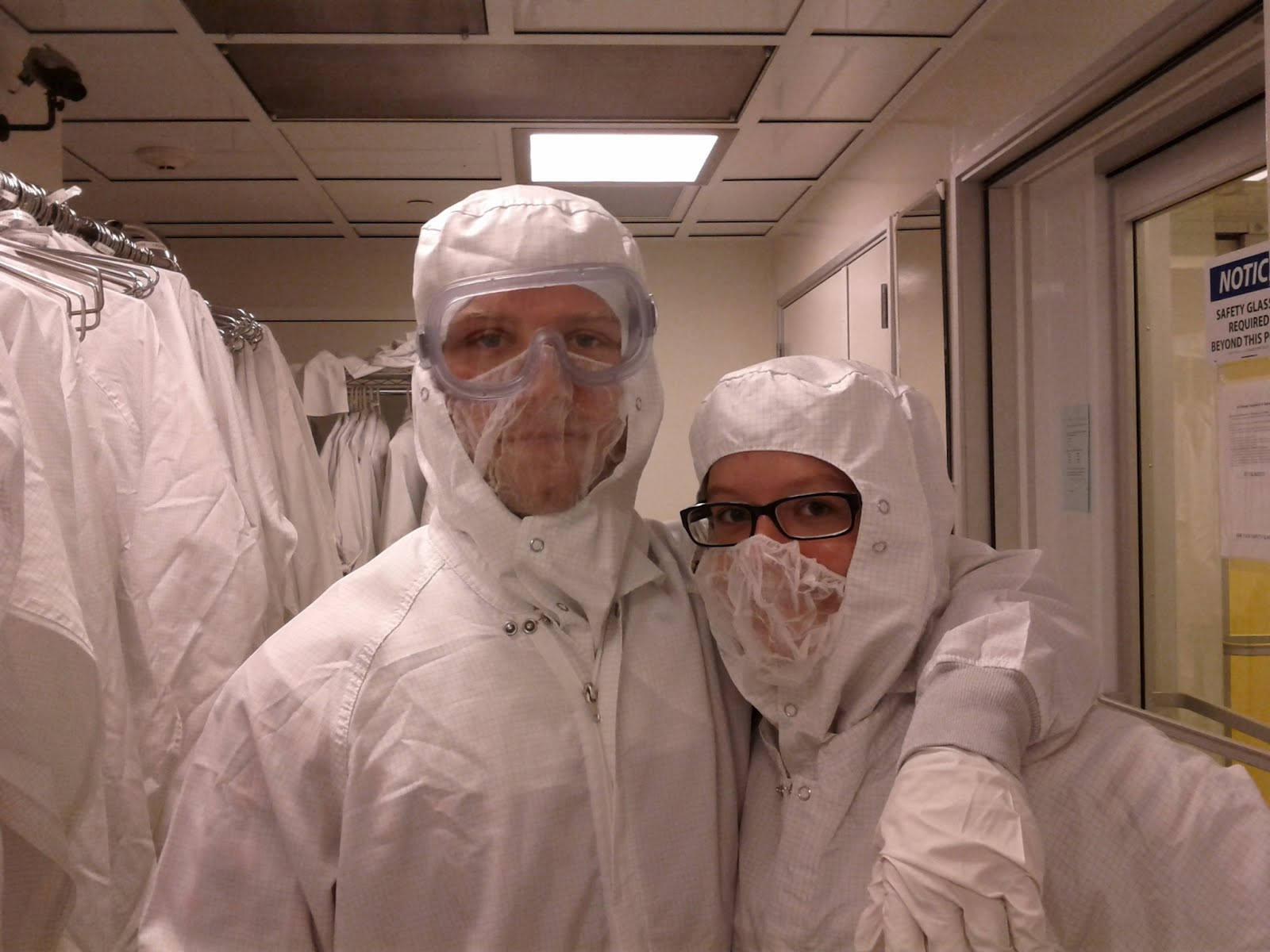
What is a cleanroom and why do you wear these funny white overalls?
Ever wondered how your cell phone camera sensor is build or the processor in your computer? These tiny but incredibly powerful sensors are fabricated in clean rooms, or so called fabs (short for microfabrication, the process done in cleanrooms). What is a fab? Its not just a room which is being cleaned often. You can not just enter this kind of room without preparing yourself for it. In principle it is a room which has way less dust particles in the air than every other room. In the average environment there are about 35,000,000 dust particles flying in 1 cubic meter. However, if you enter an average fab, there are only 3,500 particles in the same area! In high class fabs you will even only have about 35 particles in 1 cubic meter. Some of the questions that I'm trying to answer in this post are, how do you get rid of all the dust, how do you keep it clean and most importantly why do we need fabs in the first place?
 Why? Clean rooms in general are used to manufacture small, complicated and delicate sensors, e.g, CMOS chips (the camera sensor in your cell phone), gyroscopes (the thing that makes your screen turn on your cell phone) or computer processors. All of these sensors feature very small parts and electronic circuits. These tiny structures are usually only a few micrometer or even smaller in size, some features are in the nanometer scale, current processors have 22 nm features. The sensors are fabricated on single crystal silicon wafers, which are round thin plates with a size of 4 to 12 inch. Multilayer coating, etching and developing steps are done to fabricate these sensors. Several dozens or hundreds of sensors are fabricated at once on one of these wafers and are cut afterwards. Due to the fact, that these chips have small features one dust particle alone can block a channel, gap or pixel in the case of the CMOS. The whole chip can be ruined afterwards. Therefore, the fewer particles in the air, the better the yield from one wafer and the lower the cost.
How to achieve a clean environment? Clean rooms are expensive facilities used in industry, research facilities or universities. The basic idea of a clean room is to have a constant air flow coming from the ceiling going straight down to the ground. In high end fabs, the floor is made from tiles with tiny holes, so air can flow through. This way any dust particles which happen to flow in the air are forced downwards and will be sucked by the ground. Another method is to suck the air from the sides in the floor. Of course, the air which is blown from the ceiling needs to be filtered first, so no particles are blown in the room at the first place. Once you have a clean environment, several procedures need to be taken to maintain the cleanliness. The air flow in the fab is crucial, therefore you shouldn’t move too fast in a fab, as dust particles on the floor might be whirled up.
What are the precautions to take before entering a clean room? Humans bring in most of the contamination into a fab, all the dust from your clothes will ruin the clean room. Therefore, you need to wear a hairnet, a mouth protection, a hood, gloves, shoes and a protective overall. Depending on how 'clean' the clean room is, you’re now ready to enter the clean room. However, if you’re about to enter a class 100 fab (cleanroom category indicating less than 3,500 particles per 1 cubic meter), you need to do much more than that. Intel e.g. has a 42 step protocol on how to enter a clean room. One of these steps is to drink a glass of water before entering the fab to clean the throat from any dust, incredible right? Additionally, regular paper, make-up and mechanical pens are not allowed. Some fabs also have a small room which you have to enter first in which all excess dust particles on your body will be blown away by strong air nozzles, it’s like taking an air shower to clean yourself. This is how you might look like before entering a cleanroom. The picture on top shows my brother and me inside the clean room facilities at the Kavli Nanoscience Institute at Caltech, USA.
Why do most clean rooms look yellow? One main procedure done in fabs is to perform photolithographic steps. It’s similar to taking pictures and developing them in a dark room. However, the wafers will be coated with a photoresist first, which is a light sensitive liquid. Subsequently, a transparency mask with your desired features is laid on top of the wafer and the wafer is exposed to light. Depending on the type of photomask the photoresist will be hardened. Afterwards, you can develop the wafer and the uncrosslinked photoresist will be removed. As the photoresist is light sensitive, yellow light is installed in some parts of the fab, because the photoresist is only sensitive to white light and will not develop under yellow light.
Overall, clean rooms are awesome and very useful. Without them, we wouldn’t be able to fabricate better, smaller and faster processors.
Subscribe to:
Posts (Atom)